Last year, the Semiconductor Industry Association (SIA) reported record sales of $439 billion for the global semiconductor industry. However, the COVID-19 pandemic has made global supply chains extremely unstable, as illustrated by the tightening supply of semiconductor chips.
As an emerging technology of the 21st century, can sla 3D printing enhance the supply chain resilience of a core component of the modern technological world? I spoke with Scott Green, chief solutions officer at 3D printer manufacturer 3D Systems, to learn more.
Currently, automakers such as Ford, Toyota and Nissan are having to scale back production because the availability of silicon microprocessors is proving to be a manufacturing bottleneck. The shortage of semiconductor chips alone is expected to delay the production of approximately 1 million vehicles in the first quarter of 2021 alone, according to data released by data company IHS. Not only the automotive industry, but game console OEMs such as Microsoft and Sony have also experienced severe inventory shortages in the past year.
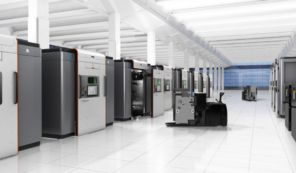
3D Systems And Wafer Fabrication Tools
3D Systems’ work in the semiconductor market began before the company acquired Belgium’s LayerWise in 2014. Prior to the acquisition, the sls 3D printing service provider was already working closely with semiconductor companies in and around Eindhoven. The knowledge brought by this acquisition has allowed 3D Systems to establish a center of semiconductor expertise in Leuven, which now works with semiconductor tool manufacturers to 3D print optimized wafer fabrication tools.
“What’s really interesting for us is seeing the adoption of Metal AM components in semiconductor fabs and being able to witness the technology advancements that impact automotive and smart device manufacturers,” Green said.
Wafer fabrication tools are the semiconductor industry’s manufacturing equipment that enable everything from microprocessors to RF amplifiers and LEDs. It includes a variety of lithography and chemical processing equipment used in series, including oxidation equipment, epitaxial reactors, vapor deposition systems, and etching equipment. Most tools involved in multi-step processes are designed to deposit or remove material from a wafer. The entire process can take up to 13 weeks, depending on the electronic device being manufactured.
Major tool OEMs such as ASML, KLA and Lam Research are primarily involved in low-volume, highly specialized parts. Rather than pumping out as many parts as possible, they are more focused on improving the quality of the parts and the efficiency of the manufacturing process in an effort to increase productivity and increase output. For reference, large fabs can produce up to 100,000 wafers per month, so increasing productivity by just 5% can produce thousands of additional semiconductor devices.
Green believes this is a great opportunity for 3D Systems’ direct metal printing (DMP) powder bed fusion technology to help. He explained: “For metal 3D printing, when you want to produce millions of parts, the cost is too high. We will not print low-demand mass-market heat sinks, but for low-volume, highly complex components and components such as semiconductor wafers Tools like factory equipment are perfect. This is a DMP application.”
Benefits Of DMP 3D Printing
DMP additive manufacturing is not only an alternative production method but also brings a series of benefits. First, the technology is well suited to geometry optimization, which means entire components can be merged into a single lightweight monolithic structure. Since available space is at a premium, overall system complexity can be reduced, and the machinery with printed parts can move faster than traditionally manufactured machinery, speeding up the entire fab production process.
Green added: “DMP will probably always be a very active topic for semiconductor processing tool companies. You need a super clean environment; you need to have the purity of materials and final product and the complexity of the geometry that DMP technology provides “Your critical components also need to be thermally optimized to ensure low thermal gradients and maximum heat dissipation where needed.”
In addition to improving performance, DMP can simplify the supply chain. For example, photolithography systems are very complex, with thousands of parts and complex assemblies. Therefore, geometric simplification can help bypass the large supply chain of integrators and subsystem assemblers. By eliminating the need for processes such as brazing, welding, assembly and sheet metal casting, 3D printing fab processing tools can potentially reduce manufacturing costs. The technology also enables faster design iterations during early development and accelerates time to market for semiconductor systems.
It’s fair to say that 3D Systems alone may not be enough to solve the current shortage of semiconductor chips, but when it comes to fab mold optimization, it can help. Following its success in Europe, the company intends to expand its semiconductor processing tools operations into the Bay Area and countries such as Japan and South Korea, where the broadest opportunities for process improvements exist.
For more information about 3D printing, please stay tuned to 3-di.Com. As a professional 3D printing service provider, Wonder 3D provides customized services such as 3D data collection, industrial design, reverse engineering, 3D printing, and post-processing of parts. It also provides plastics, photosensitive resins, nylon powders, metal powders, paraffin, etc. Including more than 20 kinds of 3D printing materials, which can meet all customers’ 3D printing service needs. For more details about Wonder’s 3D printing services, please click here https://3-di.com/guide/ to learn!