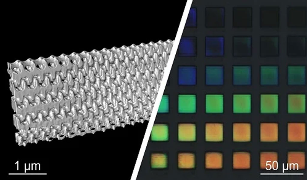
Nanoscale 3D printing technology is also an important development direction of 3D printing technology, especially in the field of electronic printing products. Nanoscale manufacturing processes are of very high value.

At present, the mainstream process of nanoscale 3D printing is the two-photon process, that is, when two laser beams converge at one point, the curing reaction of the resin material will occur. The advantage is that complex structures can be realized in nanoscale sizes. The disadvantage is that it requires the use of two lasers and the control system is more complex, resulting in relatively high printing costs.
To this end, researchers from Karlsruhe Institute of Technology and Heidelberg University in Germany have invented a two-step 3D printing and rapid prototyping process that uses blue laser diodes and can be used in small, cheap printers.
The principle of the two-step 3D printing process is to first irradiate the material with a beam of laser to make the irradiated area in an intermediate state, and then irradiate it with a laser beam to convert the intermediate state into an excited state. It can be said that two-photon realizes nanostructures from the spatial dimension, while two-step 3D printing realizes nanostructures from the time dimension.
The researchers said that two-step resin,nylon and metal 3D printing requires a special photoresist, and they have now worked with chemists to develop a photoresist. Researchers said that compared with the two-photon 3D printing method, two-step 3D printing has the advantages of low laser power, simpler structure, convenient control, and lower cost. Especially in terms of cost, the cost of the two-photon system is much more expensive than the two-step 3D printing system.
